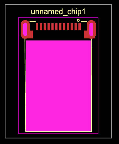
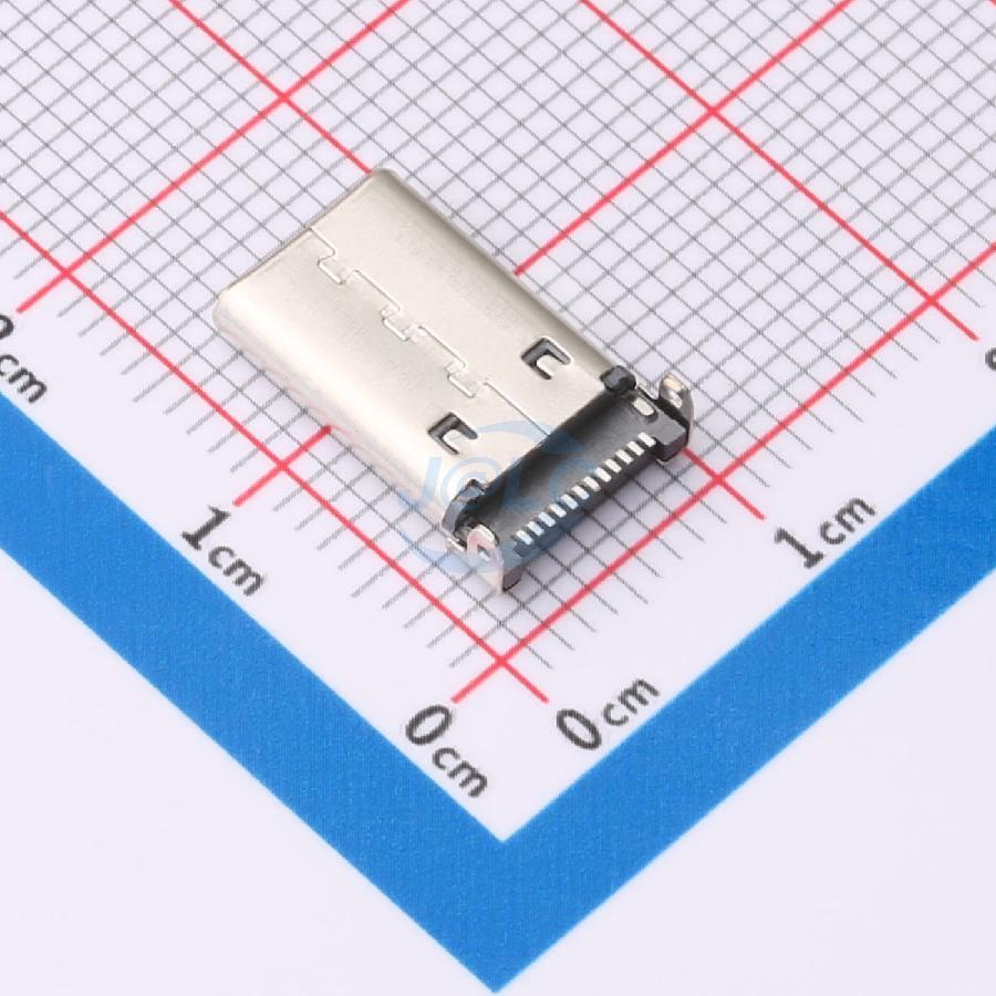
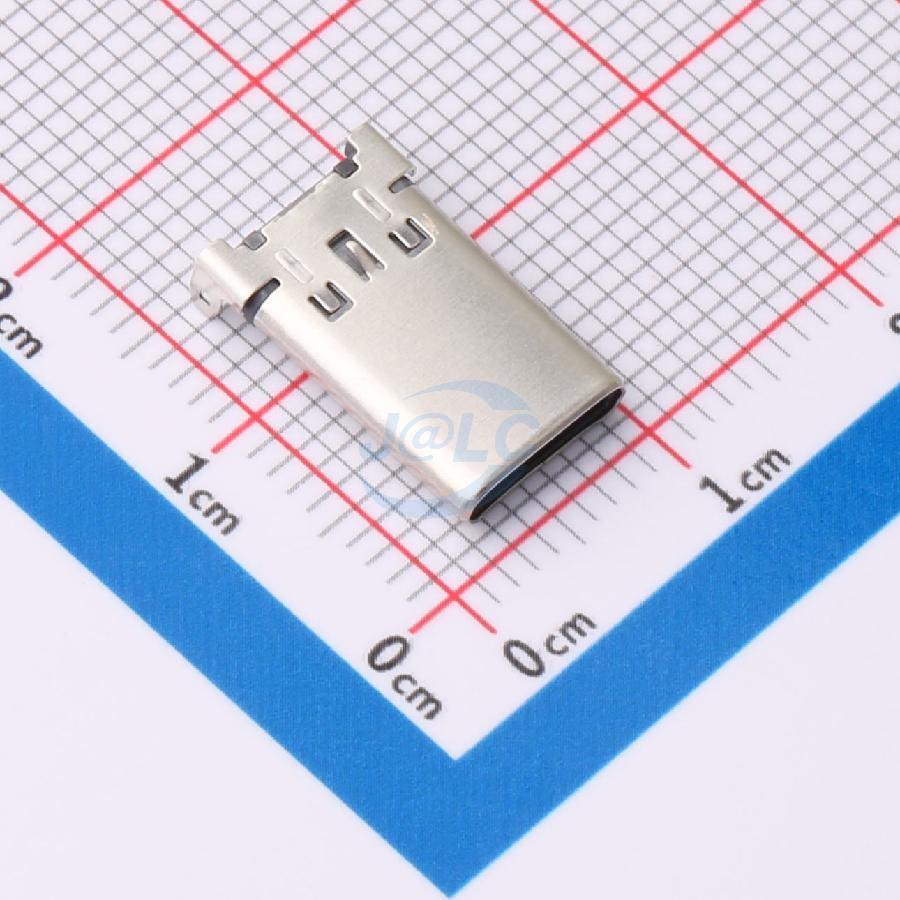
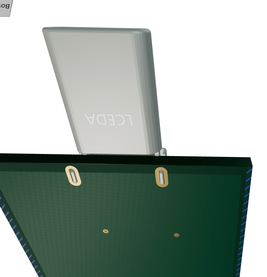
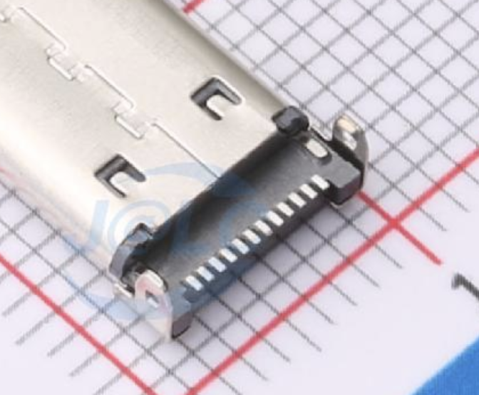
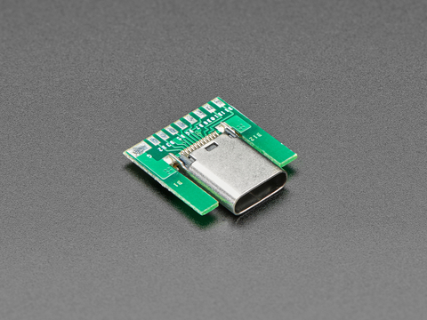
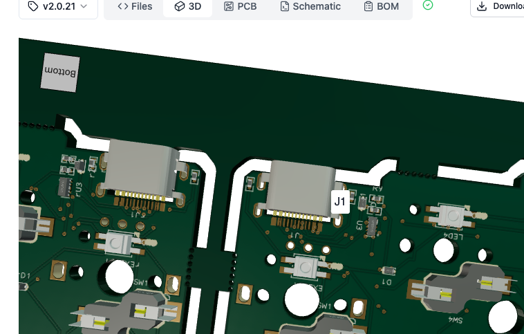
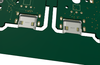
Its merged now, so to fix my current board do I need to give it any specific prompt ?
R
Rishabh
It should be upstream, you can ask ai to re-import that component. And you should see the cutout in the pcb board
pixalynx
Hey guys this is the response i got back from jlcpcb
```We have checked with our engineering team, but unfortunately, we have not found a suitable drop-in replacement for J1 (C2879827) that meets your requirements without modifying the PCB.
Could you please confirm how you would like to proceed?
Provide your own replacement component for us to use for assembly; or
Leave J1 as DNP (not assembled).
Please note that if J1 is left as DNP, the unused component will not be shipped together with the finished boards.
We will not modify the PCB or force-fit the original connector without your approval.
Please let us know your preferred option, and we will proceed accordingly.
Thank you for your understanding and support.
Best regards,
Mason```
Not sure what the best way to proceed
pixalynx
should i let them modify the pcb ?
R
Rishabh
ask them to cancel the order. You can re-order that board with the new cutout in place, which will work
pixalynx
ok
Seve
<@809856037376491570> might not be a full refund since they already have fabricated and partially assembled, my guess is he'll get back just shipping
Seve
you could ask it to be force-fit <@174613218772254720> haha
Seve
idk
Seve
rishabh is probably right that cancelling is the best option
Seve
if they'll do it
R
Rishabh
Is it? I think if you nudge them couple of times they might refund the full amount
Seve
worth a try
R
Rishabh
yeah
pixalynx
if we go the force fit route, what are the implications ?
R
Rishabh
It might break or get uprooted from the pcb while plugging in the usb cable to it
Seve
i'm not sure it's possible in this case haha
Seve
they'd need to dremel the pcb
pixalynx
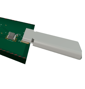
Hey guys can i get a review on v1.2.6 - https://tscircuit.com/pixalynx/esp32-usb-ducky#3d I think it has the usb connector better placed however in the 3d viewer there is a slight gap from the pcb edge, is this ok/expected ?
pixalynx
Also was there a new tscircuit update? my traces are looking soo much cleaner in v1.2.6 vs the v1.2.4(this is what went to jlcpcb)
R
Rishabh
I don't think it's still imported using the latest easyeda-converter
R
Rishabh
cause I don't see the cutout yet
R
Rishabh
or maybe it's okay
R
Rishabh
I think this is what expected, the usb c shouldn't be placed on top of the board rather in between the cavity.
<@757706909351411845> what should we do in this case? cause the easyeda-converter has the cutout in place, but that is for the metal part.
are you sure about that ^ ?because from the iamges it looks like it just hangs off the board 😱
pixalynx
from the jlcpcb images
R
Rishabh
I think so, this is one of my board which I have sent for fab. I haven't received any complaints from the fabricator.
https://tscircuit.com/imrishabh18/corne-keyboard#3d
ill just use your project and take the usb connector and put it in mine ? that should work
R
Rishabh
That's usb-c female, you plug a usb-c male to this
pixalynx
oh
pixalynx
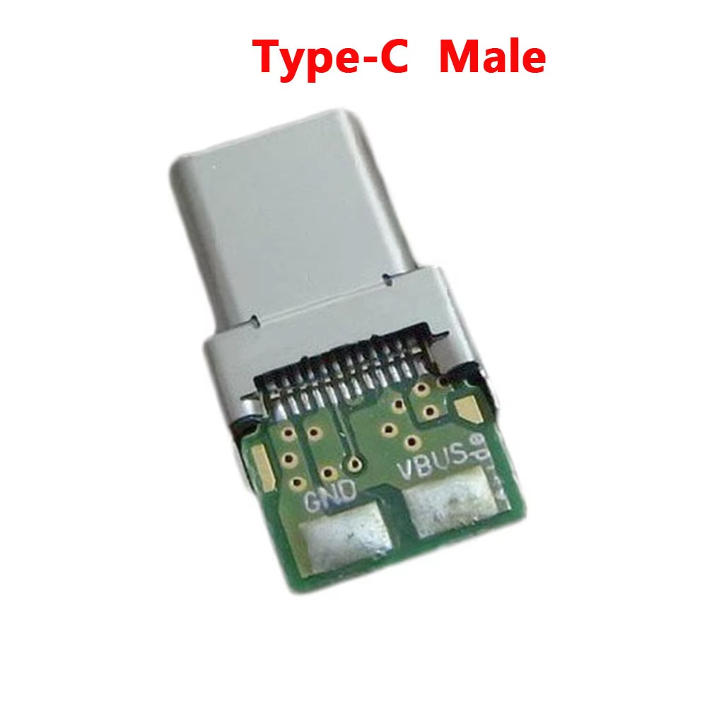
mine was usb c male
pixalynx
have you guys previously sent a usb c male for fab before ?
R
Rishabh
I don't think so
R
Rishabh
Ask claude for reference kicad files for the board which you're trying to make. Or ask the ai what is the best way with the cavity or without.
pixalynx
I havent replied to them for the previous message(been busyh with work) but they just sent me this email
```We have further checked with our production team, and they have confirmed that J1 (C2879827) can be reworked.
However, please note that the rework process involves certain risks to the PCB and connector, so we would like you to be aware of this before proceeding.
If you would like us to proceed with the rework, please provide us with the updated and complete production files for our review and confirmation.
Once we receive the updated files, we will continue to evaluate the rework arrangement and proceed accordingly.
Thank you for your understanding and cooperation.
Best regards,
Mason```
R
Rishabh
I think you can try and send the new fabrication file's and see what they say
pixalynx
ok
pixalynx
send them the new fab files, let see what they say 🤞
pixalynx
Hey guys this was the latest update from JLCPCB ```Hi Customer,
Thank you for providing the updated fabrication files.
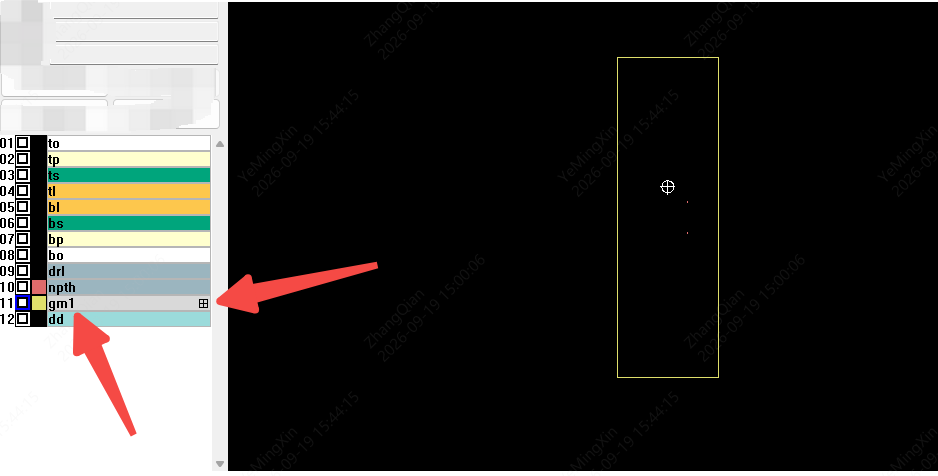
For the revised PCB design, please move the board outline to the mechanical layer (GM1), as shown in the picture below.
After updating the file, please send us the revised fabrication files so we can proceed with the review.
Thank you for your cooperation and support.
Best regards,
Mason```
i think maybe your AI might have done something weird to export the gerbers
Seve
i don't see any obvious issues
Seve
when you uploaded gerbers, were those the jlcpcb gerbers? Or did you regenerate?
pixalynx
Can you run it on v1.2.6 because v1.2.4 is the version that went to jlcpcb for initial fab where it had the usb c placement error.
v1.2.6 is the one where i re ran and it had fixed the usb type c placement and i sent the fab files via email and not through the jlcpcb ui
Seve
i think you should send the screenshot of the JLC feedback to your AI for correction
Seve
i'm not 100% sure it's a tscircuit bug since thisis the first time i've seen it
Seve
it seems more likely to me that your AI manually generated gerbers or something weird like that
pixalynx
ok let me have a look
pixalynx
```Let me look at the actual layer files in that export to pin down what their CAM is complaining about.
Inspected layer naming and outline file content
Now I can explain exactly what's happening, and it's a file-naming problem, not a design problem.
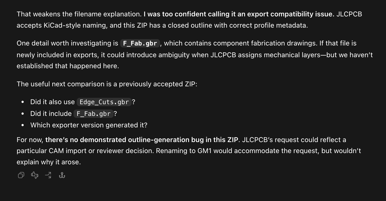
Your outline file is correct in content: Edge_Cuts.gbr holds the closed rectangle (x -13..13, y -49..33.25) drawn with a 0.05 mm aperture, and it even declares itself properly with the Gerber X2 attribute %TF.FileFunction,Profile,NP. Their CAM ignores that attribute and maps layers by filename, which is why the outline never reached the GM1 slot.
Let me build the corrected files.```
pixalynx
```Corrected bundle built — same copper, outline now named .GM1. Updating the project's fab script so future bundles comply too, and sending you the file.
Updated fab script for GM1 and rebuilt 1.2.8 bundle
Sent
v1.2.6 with JLC's fix applied: the exact files you already sent, with the outline renamed Edge_Cuts.gbr → esp32-usb-ducky.GM1 and F_Fab.gbr removed. No copper, drill, BOM or CPL changes.
ZIP
esp32-usb-ducky_v1.2.6_GM1.zip
52.1KB
What Mason is asking for: their CAM can't find your board outline, so they want it supplied as the mechanical layer GM1.
Why it happened — a naming issue, not a design one:
Your outline file is correct inside. Edge_Cuts.gbr holds the closed rectangle (x -13..13, y -49..33.25) drawn with a 0.05 mm aperture, and it declares itself properly with the Gerber X2 attribute %TF.FileFunction,Profile,NP.
Their CAM maps layers by filename, ignoring that attribute. The screenshot's 12 rows match your 12 files exactly: to/tp/ts/tl = top silkscreen/paste/mask/copper, bl/bs/bp/bo = the bottom set, drl/npth = your two drill files. That leaves gm1 and dd for the two files their matcher didn't recognise — Edge_Cuts.gbr and F_Fab.gbr.
So the slot they rout the board from is holding the wrong file, which is why the layer they highlighted looks nearly empty.
F_Fab.gbr is worth removing rather than renaming. It's a fabrication drawing of component outlines spanning x -10..11.8, y -47.5..15.9. If an operator ever treated that as the mechanical layer, it would rout along part outlines instead of the board edge.
The fix, in the file I've sent you: the exact files you already sent them, with Edge_Cuts.gbr renamed to esp32-usb-ducky.GM1 (byte-identical content, verified) and F_Fab.gbr dropped. Copper, drill, BOM and pick-and-place are untouched, so it's still the v1.2.6 design they're mid-review on — nothing for them to re-check but the outline.```
pixalynx
that was the response from claude, i think its good for me to resend the newer files
Want to add to the conversation?
Reply in Discord so your notes stay connected to the source.