astrimid - Regarding multiple components in one...
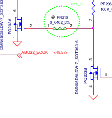
Regarding multiple components in one body. Another detail directly relevant to manufacturing (but probably not for schematic purposes) is an ability to split one physical component into A and B part. In this example, PQ203 is a dual MOSFET, meaning it's two independent <mosfet in
Regarding multiple components in one body.
Another detail directly relevant to manufacturing (but probably not for schematic purposes) is an ability to split one physical component into `A` and `B` part. In this example, PQ203 is a dual MOSFET, meaning it's two independent `<mosfet>` in one PCB body. So pins have continuous numbering across the multiple components in a schematic.
This is probably the hard one, as you'd need two different view for schematic and PCB trace:
for PCB you must have it as a single chip, while for schematic you'd want A part and B part:
```
{/* Physical Dual MOSFET package placed on the PCB */}
<chip name="PQ203" footprint="soic8" />
{/* PART A: Positioned on the left side of the schematic sheet */}
<mosfet
name="PQ203A"
schX={-15}
schY={10}
connections={{
gate: "net.gate_ctrl_A",
source: "net.gnd",
drain: "PQ203.pin8" // Tied to physical pin 8 of the single chip
}}
/>
{/* PART B: Positioned far away on the right side of the schematic sheet */}
<mosfet
name="PQ203B"
schX={25}
schY={-5}
connections={{
gate: "net.gate_ctrl_B",
source: "net.gnd",
drain: "PQ203.pin5" // Tied to physical pin 5 of the single chip
}}
/>
```
A
astrimid
Don't know if it's possible to hide the `chip` component for schematic, while hiding A and B components for the PCB and still representing these two components as in one physical body. I guess it can be thought of internal implementation of a chip flattened to a schematic.
Maybe something like this:
```
<DualMosfet
name="PQ203"
// Position Part A near your power entry logic
partA_schX={-20}
partA_schY={15}
// Position Part B far away near your switching/control logic
partB_schX={35}
partB_schY={-10}
connections={{
gateA: "net.gate_ctrl_A",
sourceA: "net.gnd",
drainA: "net.vcc_switched",
gateB: "net.gate_ctrl_B",
sourceB: "net.gnd",
drainB: "net.led_driver",
}}
/>
```
Or maybe this could be a group/subcircuit/chip with ports?
Seve
hmmm that's interesting and yes i think DualMosfet makes sense
Seve
the mosfets would be represented with a spice model that contains two mosfets right?
Seve
it's kind of like a mosfet array
A
astrimid
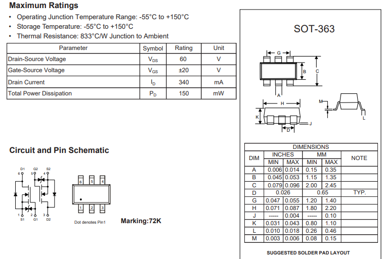
I've looked at DMN65D8LDW manufacturer's SPICE model, and contains only one MOSFET. Additional components in the model provide specification for timing, body diode, resistance, but not the second transistor. So semantically it's 2 MOSFETs in one body.
Does tscircuit already have an array of component packed into one physical chip/group, while specifying properties for each so that they could be split into different parts of the schematic?
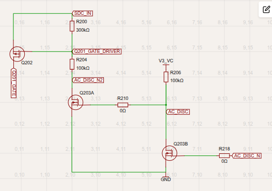
schematic of AC_DISC path.
PQ203A and PQ203B are inside DMN65D8LDW 6 pin chip.
There's a separate use case where DMN65D8LDW has both mosfets acting as one, even though it's 6 pin package.
BTW, couldn't find the sot363 in the footprint list. Maybe footprint should be provided in the `<chip>` while the schematic level mosfets should not required `footprint`.
yea schematics should run without footprints specified for sure
Seve
CC <@809856037376491570>
A
astrimid
I've tried it, and it looks like this is already possible with custom components and chips:
```
<DualMosfetSot363
name="Q203"
mfg="Diodes Inc."
mpn="DMN65D8LDW"
footprint="sot363"
chA={{
channelType: "n",
mosfetMode: "enhancement",
symbolDrainSide: "top",
symbolSourceSide: "bottom",
symbolGateSide: "right",
schSectionName: "ac_disc_path",
schRotation: 0,
schX: 2.3,
schY: 13,
}}
chB={{
channelType: "n",
mosfetMode: "enhancement",
symbolGateSide: "right",
schSectionName: "ac_disc_path",
schX: 6,
schY: 11,
}}
/>
```
The tricky part is how to specify that `<mosfet>` is inside the `<chip>` rather than connected to it exteranally, while also maintaining the ports mapping and separate A/B channel coordinates, and passing throught all those properties.
A
astrimid
Maybe there should be some kind of composition relationship between chip and implementation? Maybe I'm missing something basic. What I need is a physical chip in 6-pin package to look like two 3-pin mosfets in schematics, while being opaque 6-pad on PCB. And also supporting loading up spice models for simulation behaviour.
A
astrimid
maybe I should use `schematicDisabled` on a `<chip>` and some kind of `pcbDisabled` on the `<mosfet>`? while also supplying a custom spice model
Seve
yea i'm trying to think this through as well
Seve
it's a case where the PCB diverges from the schematic right
Seve
i think one way to do it is sort of as you suggested, the <chip /> and <mosfet /> are BOTH defined, but are somehow linked together e.g.
```
<chip name="U1" footprint="soic8" />
<mosfet chipRef="U1" name="Q1" />
<mosfet chipRef="U1" name="Q2" />
```
but i think that's a bit unclear
```
<chip name="U1" footprint="soic8" />
<mosfet footprintRef="U1" pinMapping? />
<mosfet footprintRef="U1" pinMapping={{ drain: "U1.pin5", ... }} />
```
A
astrimid
I think what nags me is whether the `<chip/>` is an opaque IC we don't know nothing about and just declare a part number as an opaque box to have a footprint on PCB and pin headers on schematic, or is it a shell for internal schematic components that expose ports through that shell.
A
astrimid
right now, as I understand `<chip/>` is an opaque box, so if we define boh chip and internal components, both would show up in pcb, schematic and simulation.
A
astrimid
Ideally, I think a new component, e.g. `<chipShell />` or some kind of `<footprint />`, should wrap the internal schematics. I saw somewhere an example of using `<port >`, but it looks like this is for logical subcircuits and groups, not for physical package having internal schematics.
A
astrimid
how about using child components? This is defining declaratively what the semantic meaning is without imposing any implementation:
```
<chipShell
name="Q203"
footprint="sot363"
mpn="DMN65D8LDW"
manufacturer="Diodes Inc."
>
{/*
2. Break out and position Subunit A
You can place it exactly where it belongs in the 'ac_disc_path' section.
*/}
<mosfet
unitId="A" // 👈 Unique subunit key (Translates visually to Q203A)
channelType="n"
schSectionName="ac_disc_path"
symbolGateSide="right"
schX={2.3}
schY={13}
schRotation={0}
pinMapping={{ gate: "pin2", source: "pin1", drain: "pin6" }}
/>
{/*
3. Break out and position Subunit B
This part can be moved to an entirely separate area of the schematic canvas!
*/}
<mosfet
unitId="B" // 👈 Unique subunit key (Translates visually to Q203B)
channelType="n"
schSectionName="power_regulation_path" // Can belong to a different visual section!
symbolGateSide="left"
schX={45}
schY={-8}
schRotation={180}
pinMapping={{ gate: "pin5", source: "pin4", drain: "pin3" }}
/>
</chipShell>
```
A
astrimid
The question is whether you use `.Q203.B.pin1` or `.Q203B.pin1` or `.Q203.pin4` to define traces
A
astrimid
concatenating chipshell name and unitId feels simpler to implement and helps with schematic subunit naming, `Q203.pin4` feels honest about physical reality while creating a bit of confusion when it's rendered to two units, `Q203.B.pin1` is idiomatic, but I've not seen examples with two dots so far. Maybe unitId property should have a full name, e.g. `unitId="Q203B"` which creates a bit of duplication, but explicit without conventions and flexible if you want a different label. So tracing becomes .Q203B. But what about pin numbers? Do we use internal or external numbers/labels? Maybe we use internal logical names, e.g. `.Q203B.gate` but provide an outer shell pin numbers on a schematic/PCB?
A
astrimid
claude wrote this spec from this thread: https://claude.ai/public/artifacts/669c2734-c2c9-4afc-8e9b-3c4fee49858e
it made some decisions I wouldn't make but maybe it has a better mental what suits tscircuit or I need a better prompt.
A
astrimid
I probably don't need the PCB part, and I currently don't need complex simulations that require custom spice models, generic mosfet is fine for my use case. But having a peace of mind that I can make a mental map from the schematic to a physical device would be nice.
A
astrimid
Maybe I just need a type of `<subcircuit/>` with different semantic and pin/port mapping mechanics. Maybe some rules can be applied to child components via TS interfaces:
- It must be inside a <chipShell> to receive a unitId; a bare <mosfet unitId="A"> outside a shell is an error.
- It must specify pinMapping, mapping its own logical terminals (gate/source/drain, or anode/cathode, etc.) to package pin numbers of the shell.
- Children behaves as a completely normal standalone components and everyting that works inside subcircuit works inside `<chipshell>` with some parent guided tweaks.
So the POC is just API to define unit identification, parent/child relationship, and redefine pin numbering (if tscircuit supports displaying pin numbers on schematic). Whether it's implemented by using high-level subcircuit/chip/disableSchematic props or internal tscicuit API can be decided down the line.
Sorry for spamming the thread. I hope it will be useful.
yes that makes sense to me, <compoundchip> or something, or possibly we just make it so that <chip> supports it whenever there is children, we could also have e.g. <schematicrepresentation> within chip
I don't fully understand the unitId concept
A
astrimid
TL;DR, unitId is all about identification and mapping.
You need to identify both the chip and the schematic inside it. To allow schematic to be positioned in different logical places on a schematic you need to identify those schematic units.
The convention is A and B appended to the name of the chip name/id. We also need to map internal logical names to the outer shell pins sorta like subcircuit ports.
```
<chipShell name="Q203">
<mosfet unitId="A" pinMapping={{ gate: "2", source: "1", drain: "6" }} />
<mosfet unitId="B" pinMapping={{ gate: "5", source: "4", drain: "3" }} />
</chipShell>
```
`<chip/>` having children makes sense, my first thought was why do you need chip, subcircuit and group, as they seem to mean the same thing. Now I see there's a need to separate traces on the motherboard and logical "traces" (connections) inside the chip.
Currently, tscircuit is about designing PCBs, as I understand, so breaking out chip internals might be pulling it in the wrong direction. Alternatively, it could keep the opaque <chip/>, but it would make them programmable, e.g. actual code that takes power line, input ports and converts them to output ports or simulation result. This would allow for more powerful firmware simulations, but it's a totally other can of worms.
A
astrimid
If `<chip>` children have automatic naming like `${chipname}${alphabetical letter}`, this could work too, it's just a bit implicit which is harder for learning curve.
M
Mustafa7
<@757706909351411845> How's this?:
```<chip name="Q203" footprint="sot363">
<schematicunit
unit="A"
symbolName="mosfet_n_channel"
pinMapping={{ gate: "pin2", source: "pin1", drain: "pin6" }}
/>
<schematicunit
unit="B"
symbolName="mosfet_n_channel"
pinMapping={{ gate: "pin5", source: "pin4", drain: "pin3" }}
/>
</chip>```
Let me know where it can be improved
we can't introduce any terms that aren't an industry standard- i haven't heart of a schematicunit before- likewise w/ unitId, unit isn't really a term we're allowed to build off
Seve
the <chip> can contain a <mosfet>, that is using standard industry terms, and makes sense
Seve
<chip>
<chipschematic>
<mosfet>
also uses standard industry terms
Seve
the api for tscircuit should be "guessable", you can use AI to suppose what the ai would be, but if you think about the implementation too much (which I think people are doing in this thread) then you become biased towards the implementation and not towards the ideal API
Seve
we start from the API not the implementation
Seve
Do this 10 times with AI, in different chats, do not give it context
6th looks good ig? similar to cadModel. What do you think?
Seve
the "collapsed" concept is good
Seve
but we prefer booleans
Seve
i would say internal/external is usually confusing
Seve
"internal to what?"
Seve
but yea actually
Seve
maybe it's ok
Seve
<internalcircuit> makes sense to me
Seve
fwiw cadModel also has <cadmodel>
M
Mustafa7
So 6th is good to go right? should we start imp?
Seve
i'm worried that <internalcircuit> might be unclear because it only contains a schematic representation.... but yea let's try it
Seve
CC <@778624824875941908> this is interesting for SPICE representation
A
astrimid
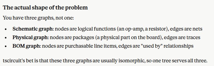
I think it's not about the specific example of dual mosfet in one package. I think it's about API to define the logical/physical split explicitly where it's needed. tscircuit has 3 models in one react element: one schematic symbol, one PCB footprint, on BOM. entry The issue arises when 1-to-1 relationship breaks.
A
astrimid
It's more of a problem of single model vs multiple views
Whad do you mean by "industry starndard"?
ASMEY14.44 defines reference designators which has units and sub-assemblies
https://en.wikipedia.org/wiki/Reference_designator
A
astrimid
If you're open to abandoning one-to-one approach:
```
<View target="schematic">
{/* schematic-only content */}
</View>
<View target={["pcb", "bom"]}>
{/* physical + BOM content, no schematic presence */}
</View>
```
Still needs cross-referencing.
A
astrimid
tscircuit already defines connections/nets (logical/PCB labeling) and traces (physical implementation). Some properties are prefixed with `sch`, some with `pcb`. So it's already split at the props level if not at element level.
Seve
Taking a look
Seve
We’re not strictly isomorphic- but we do think about modular representation and yes for sure we think about explicitly designated for things to render “only in schematic” or “only in pcb”
Seve
But we also think about the natural expression, and redundant representation- eg repeating <mosfet ref=“.U1 internalcircuit .Q1” />
A
astrimid
One approach that could provide this flexiblity is ability of user-defined custom elements to implement circuit JSON directly. This way users can specify fine grained circuitjson representation using user defined <PCBDevice> and <SchematicUnit> elements (names are just an example) that work in the editor playground. Maybe it could be implemented using some react hooks/context API.
A
astrimid
I think tscircuit needs an **escape hatch** for use cases where basic assumptions break, use case is pecurliar and API is not yet available. Currently, PCB and schematic are fighting each other: sometimes you want to assign sourcing and physical pins to schematic elements, sometimes you want to wrap schematic elements with PCB device.
The fundamental problem with **React** model is that it's a **tree**, while circuits is multiple **graphs** (physical graph and logical graph) and bidirectional relationship between them. `<net>` and `<trace>` work for defining network graphs, but when the components themseves need **composition** relationship, the abstraction over circuitJSON database leaks.
When we design PCBs, we want **logic-first** approach: define how the system works semantically, then assign manufacturers and sourcing, tweak generated PCB, adjust sourcing to optimize cost. When we analyze PCBs, we want **physical-first** approach: define the physical traces and footprints, explode schematic of chips and define simulations. And engineers often switch back and forth between **top-down synthesis** and **bottom-up analysis**.
Back to our example of dual mosfet:
- synthesis: logical function -> high side mosfet + low side mosfet -> implement as a chip + PCB
- analysis: PCB traces and chips -> extract logical function as schematic -> explode chips as schematic -> simulate with injecting voltage and monitor using scopes
So it seems exposing raw circuitjson database via tscircuit props package is the only way to provide user-driven model organization. But the problem is we still need the coordinate system be context driven as we don't want to hard code the coordinates while still preserving relational positioning and routing. So we need a mechanism to pass down low level positioning as props from high-level contexts.
A
astrimid
So for synthesis, the low level API needs to allow injecting pcb part into the circuitjson and defining the schematic representation controllable from the higher level component.
For analysis, we need to query circuitjson by id, so that we can construct a simulation bench component without modifying the model while still be able to override some parameters of the model for simulation purpose.
A
astrimid
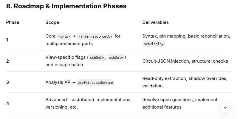
Here's an updated Claude summary/rfc of this thread that incorporates the `<internalcircuit>` and `collapsed` visibility control API from this discussion while sugesting other API levels to expose more user control. It also introduces termonology aligned with ASME/IEEE standards (element < part < unit).
https://claude.ai/public/artifacts/c87b3c8a-e757-41b6-999b-5320a0155530
This pushes tscircuit into ability to define internals of passive IC while still leaving room for drill down into SoC, microcontrollers and CPU schematics. Maybe even silicon fabrication file and chip simulation/emulation in the future.
A
astrimid
So far, `<chip>` + child nesting of schematic with display control (expanded by default, collapsible and completely hidden) seems to be a straightforward addition. Maybe pcbOnly/schOnly as phase 2 for non-nestable elements.
I wonder what's the purpose of `<constainedlayout>` with `pcbOnly` and `schOnly` props: https://github.com/tscircuit/props/pull/42
This might be exactly what's needed here
Seve
Just read through this- im not satisfied with the examples for schOnly and pcbOnly- i dont understand how this solves a problem- i think a more full ecample would help clarify what this solves. Im not inherently opposed to the props but i dont see the concrete/literal example of where they are needed
Seve
Constrainedlayout effecitvely isnt used at the moment- the api may be deprecated (some apis/layout algorithms never saw enough usage)
Seve
Also astramid i dont mean to be dismissive at all, we are at a 3 day conference otherwise i would dig in and make my own suggestions- it is solely because of limited time that im not suggesting/collaboratingbetter- i really value your feedback/ideas i think you are on to something- i just dont understand enough to greenlight schOnly/pcbOnly because it seems to me the internal mosfets are represented now
A
astrimid
are you saying `<internalcircuit>` already green lighted? or are you saying you can aleady achieve separate representations for pcb and schematic? I've tried chip + mosfet and there seem to be no way to hide chip from schematic
A
astrimid
also, I'd like the ability to view physical chip part props on "logical" elements, like real pin numbers and the manufacturer part number, but that's something for later enhancement
A
astrimid
I'm in no rush. I can find more examples of multi-element parts if that what you're looking for. Good luck with a conference
A
astrimid
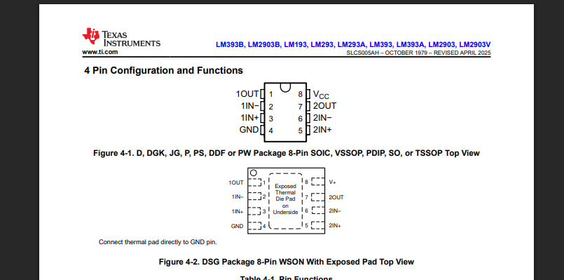
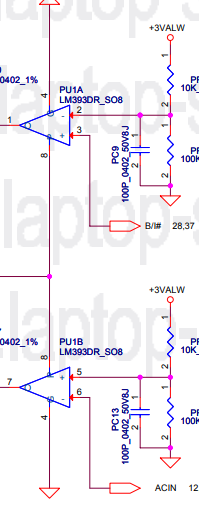
here's texas intstruments dual channel comparator in soic8 footprint, that has 2 element schematic
notably, here pin 8 and pin 4 are shared between two comparator elements, while in dual mosfets example they are logically indepenent elements
M
Mustafa7
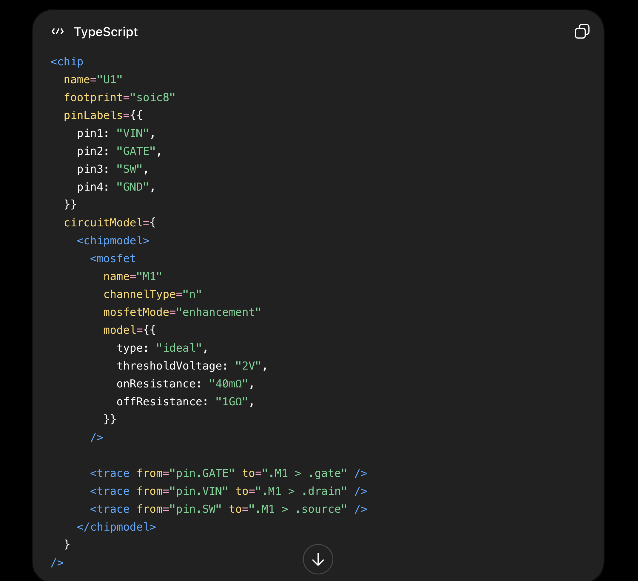
```<chip
name="Q1"
footprint="soic8"
pinLabels={{
pin1: "G1",
pin2: "S1",
pin3: "G2",
pin4: "S2",
pin5: "D2",
pin6: "D2",
pin7: "D1",
pin8: "D1",
}}
connections={{
G1: "net.GA",
S1: "net.SA",
D1: "net.DA",
G2: "net.GB",
S2: "net.SB",
D2: "net.DB",
}}
internalCircuit={
<internalcircuit>
<mosfet
name="A"
channelType="n"
mosfetMode="enhancement"
schX={-3}
schY={0}
connections={{
gate: "pin.G1",
source: "pin.S1",
drain: "pin.D1",
}}
/>
<mosfet
name="B"
channelType="n"
mosfetMode="enhancement"
schX={3}
schY={0}
connections={{
gate: "pin.G2",
source: "pin.S2",
drain: "pin.D2",
}}
/>
</internalcircuit>
}
/>```
Isn't this syntax good enough, the internalcircuit will be shown in schematic as U1A, U1B. chip will be hidden from schematic and will be shown only in pcb
A
astrimid
Yeah, it's essentialy the same as `<chip children={<internalcircuit/>} />` without nesting syntax sugar. One consideration: sinse you're already using custom property name, why not just do `<chip internalcircuit={[<element1/>, <element2/>]}` without wrapper, as `<internalcircuit/>` then won't be useful on its own.
M
Mustafa7
We are following the already used patterns as <internalcircuit/> is similar to <cadmodel/>
A
astrimid
I see. So same pattern should be applied to pinLabels and conections?
```
<chip
pinLabels={<pinLabels pin1="G1" />}
connections={<connections G1="net.GA" />}
```
Also footprint might be something more complex than just a string:
```
<chip footprint={<footprint name="soic8" width="150mil" height="50mil" />} />
```
Seve
Not all props can contain elements, but all props that accept elements can be specified as children. For stuff like pin labels or connections, these are already shorthands for port and trace concepts
Seve
It is a good thought tho- would love to elaborate more too because i love api design and making sure we’re correct- but i gotta sleep!!
A
astrimid
`<schematicbox` approach seems to work
Want to add to the conversation?
Reply in Discord so your notes stay connected to the source.